How Reverse Recovery is Calculated
There are multiple standards for reverse recovery measurements.
| Device types | Discrete Standard | Module Standard |
|---|---|---|
| IGBT, Enhancement, Si | JESD 24-10 + IEC 60747-8 setup + extra parameters | IEC 60747-2 |
| JESD 24-10 + IEC 60747-8 setup + extra parameters | IEC 60747-2 | FET, Enhancement, Si |
| JESD 24-10 + IEC 60747-8 setup + extra parameters | IEC 60747-2 | JESD 24-10 + IEC 60747-8 setup + extra parameters |
| IEC 60747-2 | FET, Enhancement, SiC | JESD 24-10 + IEC 60747-8 setup + extra parameters |
| IEC 60747-2 | JESD 24-10 + IEC 60747-8 setup + extra parameters | IEC 60747-2 |
| FET, Enhancement, GaN, vertical JESD 24-10 + IEC 60747-8 setup + extra parameters | IEC 60747-2 JESD 24-10 + IEC 60747-8 setup + extra parameters | IEC 60747-2 |
| FET, Enhancement, GaN, Cascode | No | No |
| FET, Enhancement, GaN, eHEMT | No | No |
| FET, Enhancement, GaN, GIT | No | No |
| FET, Depletion, Si | JESD 24-10 + IEC 60747-8 setup + extra parameters | IEC 60747-2 |
| JESD 24-10 + IEC 60747-8 setup + extra parameters | IEC 60747-2 | FET, Depletion, SiC |
| JESD 24-10 + IEC 60747-8 setup + extra parameters | IEC 60747-2 | JESD 24-10 + IEC 60747-8 setup + extra parameters |
| IEC 60747-2 | FET, Depletion, GaN, vertical | JESD 24-10 + IEC 60747-8 setup + extra parameters |
| IEC 60747-2 | JESD 24-10 + IEC 60747-8 setup + extra parameters | IEC 60747-2 |
| FET, Depletion, GaN, Cascode | No | No |
| FET, Depletion, GaN, eHEMT | No | No |
| FET, Depletion, GaN, GIT | No | No |
JESD 24-10
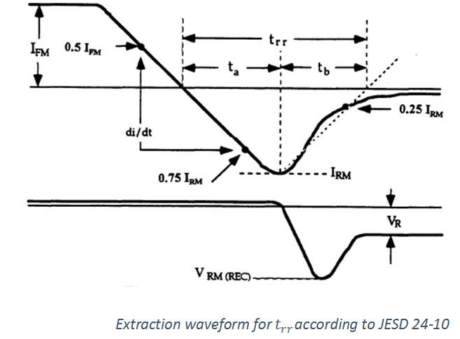
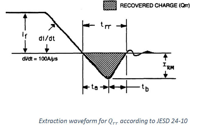
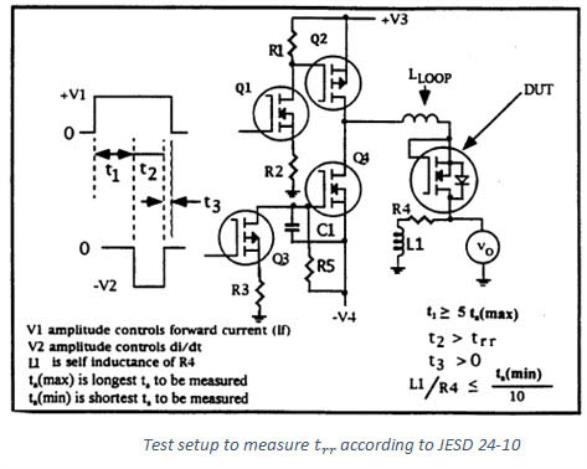
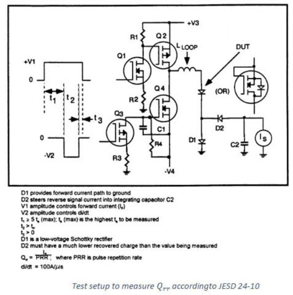
JESD 24-10 shows how to measure and extract reverse recovery time and charge of power MOSFET drain-source diodes. The standard is applicable for power MOSFETs with drain-source diodes.
Test setup
Gate must be shorted to source, therefore gate voltage is 0 V and there is no negative bias. Both ta and tb must be measured and add up to trr. di/dt is defined as 100 A/(µs) and no flexible value.
Algorithm
Notes and Keysight PD1000A deviations
- The same standard applies for IGBTs.
- We also extract ERR
- We have multiple values for di/dt as parameter and not fixed at 100 A/µs
- We allow negative gate voltages and don’t have gate shorted to source as specified in standard
- We do not measure ta and tb separately.
- PD1000A software searches for first crossings of 0 A, and first crossing of 0.25 IRM after current peak, etc.
- It is currently possible to change the 25% of IRM and use different user input for the percentage between 0% and 99%.
- The output current signal is smoothed with smoothing points = 5 before extraction. IRM is extracted with this smoothed signal.
- For other extractions (trr, charge, energy, di/dt, ti) an additional user smoothing (default of 10 smoothing points) is applied before.
IEC 60747-8
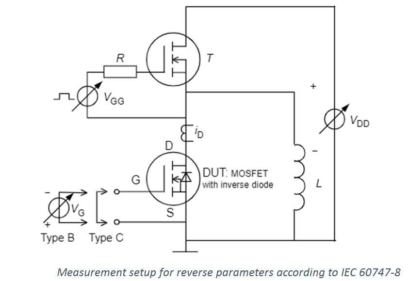
This section first describes the important parts of the IEC 60747-8 standard with regards to reverse characteristics. It then gives some notes and explains how PD1000A software adapts this standard or deviates from it. The standard is applicable for discrete FETs. These include J-FETs and both insulated-gate depletion/enhancement FETs. Applicable to n-channel types. Circuits can be adapted for p-channel types by changing polarities of meters and power supplies.
Test setup
The test setup changes slightly for depletion (type B) and enhancement (type C) transistors.
Algorithm
Notes and Keysight PD1000A deviations
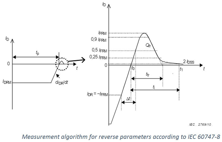
The measurement algorithm is not used in PD1000A. It is not practical as the end point of the reverse pulse is impossible to measure with an oscilloscope. We use almost the same test setup as defined in IEC 60747-8. The only change is that we allow for negative bias voltages also for enhancement transistors.
Following IEC 60407-8 for FETs, Body Diode Reverse Recovery is calculated as follows:
| Parameter, | Description, | Corresponding section in IEC 60407-8 |
| Drain current (IDSS) with gate shorted to source (VGS=0), | This is a static measurement. Therefore, it is preferably taken by the B1505A or B1506A and passed as a parameter to the DPT system., | 6.3.3 |
| Forward Recovery Time, | The forward recovery time (tfr) is measured as the interval between the time of t0 when the drain current passes through zero and the time when, for decreasing values of ID, a line passes through the points for 0.9 IFRM and 0.25 IFRM crosses the zero current axis. (IFRM = maximum reverse current), | 6.3.14 |
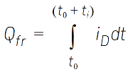
| Forward Recovery Charge Ofr, |
Integration start time t0 is the instant when the current passes through zero. Integration end time t1 is the time when the forward drain current reaches 2xIDSS, preferably equal to the specified maximum value of tfr., |
6.3.14 |
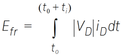
| Forward Recovery Energy Efr of Diode, |
|
Not addressed in the IEC standard |
